- 您现在的位置:买卖IC网 > Sheet目录472 > MAX2120EVKIT+ (Maxim Integrated)KIT EVAL FOR MAX2120
�� �
�
�Complete,� Direct-Conversion� Tuner� for� DVB-S�
�and� Free-to-Air� Applications�
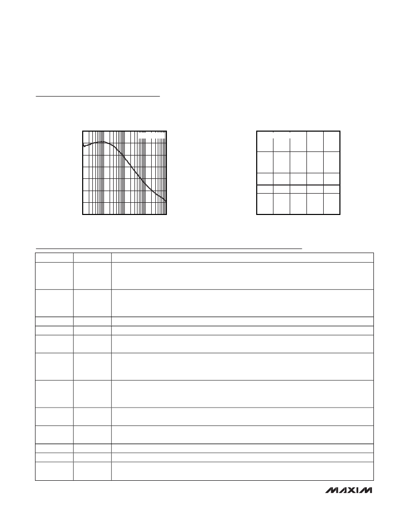
�Typical� Operating� Characteristics� (continued)�
�(MAX2120� Evaluation� Kit:� V� CC� =� +3.3V,� baseband� output� frequency� =� 5MHz;� V� GC1� =� 1.2V;� T� A� =� +25°C.� Default� register� settings�
�except� BBG[3:0]� =� 1011.)�
�PHASE� NOISE� vs.� OFFSET� FREQUENCY�
�LO� LEAKAGE� vs.� LO� FREQUENCY�
�-60�
�f� LO� = 1800MHz�
�-70�
�MEASURED AT RF INPUT�
�-70�
�-80�
�-75�
�-90�
�-80�
�-100�
�-110�
�-120�
�-130�
�-85�
�-90�
�0.1�
�1�
�10�
�100�
�1000�
�925�
�1175�
�1425�
�1675�
�1925�
�2175�
�OFFSET� FREQUENCY� (kHz)�
�LO� FREQUENCY� (MHz)�
�Pin� Description�
�PIN�
�1�
�2�
�3�
�4�
�5�
�6�
�7�
�8�
�9�
�10�
�11�
�12�
�NAME�
�VCC_RF2�
�VCC_RF1�
�GND�
�RFIN�
�GC1�
�VCC_LO�
�VCC_VCO�
�VCOBYP�
�VTUNE�
�GNDTUNE�
�GNDSYN�
�CPOUT�
�FUNCTION�
�DC� Power� Supply� for� LNA.� Connect� to� a� +3.3V� low-noise� supply.� Bypass� to� GND� with� a� 1nF� capacitor�
�connected� as� close� as� possible� to� the� pin.� Do� not� share� capacitor� ground� vias� with� other� ground�
�connections.�
�DC� Power� Supply� for� LNA.� Connect� to� a� +3.3V� low-noise� supply.� Bypass� to� GND� with� a� 1nF� capacitor�
�connected� as� close� as� possible� to� the� pin.� Do� not� share� capacitor� ground� vias� with� other� ground�
�connections.�
�Ground.� Connect� to� the� board’s� ground� plane� for� proper� operation.�
�Wideband� 75� ?� RF� Input.� Connect� to� an� RF� source� through� a� DC-blocking� capacitor.�
�RF� Gain-Control� Input.� High-impedance� analog� input,� with� a� 0.5V� to� 2.7V� operating� range.� V� GC1� =�
�0.5V� corresponds� to� the� maximum� gain� setting.�
�DC� Power� Supply� for� LO� Generation� Circuits.� Connect� to� a� +3.3V� low-noise� supply.� Bypass� to� GND�
�with� a� 1nF� capacitor� connected� as� close� as� possible� to� the� pin.� Do� not� share� capacitor� ground� vias�
�with� other� ground� connections.�
�DC� Power� Supply� for� VCO� Circuits.� Connect� to� a� +3.3V� low-noise� supply.� Bypass� to� GND� with� a� 1nF�
�capacitor� connected� as� close� as� possible� to� the� pin.� Do� not� share� capacitor� ground� vias� with� other�
�ground� connections.�
�Internal� VCO� Bias� Bypass.� Bypass� to� GND� with� a� 100nF� capacitor� connected� as� close� as� possible� to�
�the� pin.� Do� not� share� capacitor� ground� vias� with� other� ground� connections.�
�High-Impedance� VCO� Tune� Input.� Connect� the� PLL� loop� filter� output� directly� to� this� pin� with� as� short�
�of� a� connection� as� possible.�
�Ground� for� VTUNE.� Connect� to� the� PCB� ground� plane.�
�Ground� for� Synthesizer.� Connect� to� the� PCB� ground� plane.�
�Charge-Pump� Output.� Connect� this� output� to� the� PLL� loop� filter� input� with� the� shortest� connection�
�possible.�
�8�
�_______________________________________________________________________________________�
�发布紧急采购,3分钟左右您将得到回复。
相关PDF资料
MAX2121EVKIT#
KIT EVAL FOR MAX2121
MAX2130EVKIT
EVAL KIT MAX2130
MAX2140EVKIT
EVAL KIT MAX2140
MAX2150ETI+T
IC MODULATOR I/Q WIDE 28TQFN
MAX2160EVKIT
EVAL KIT MAX2160
MAX2163ETI/V+
IC TUNER ISDB-T LOW IF 28TQFN
MAX2165EVKIT+
KIT EVAL FOR MAX2165
MAX2170EVKIT+
KIT EVAL FOR MAX2170
相关代理商/技术参数
MAX2121
制造商:MAXIM 制造商全称:Maxim Integrated Products 功能描述:Complete Direct-Conversion L-Band Tuner
MAX2121_V1
制造商:MAXIM 制造商全称:Maxim Integrated Products 功能描述:Complete Direct-Conversion L-Band Tuner
MAX2121ETI
制造商:MAXIM 制造商全称:Maxim Integrated Products 功能描述:Complete Direct-Conversion L-Band Tuner 925MHz to 2175MHz Frequency Range
MAX2121ETI+
功能描述:调谐器 Direct-Conversion L-Band Tuner RoHS:否 制造商:NXP Semiconductors 功能: 噪声系数: 工作电源电压: 最小工作温度: 最大工作温度:
MAX2121ETI+T
功能描述:调谐器 Direct-Conversion L-Band Tuner RoHS:否 制造商:NXP Semiconductors 功能: 噪声系数: 工作电源电压: 最小工作温度: 最大工作温度:
MAX2121EVKIT#
功能描述:射频开发工具 MAX2121 Eval Kit RoHS:否 制造商:Taiyo Yuden 产品:Wireless Modules 类型:Wireless Audio 工具用于评估:WYSAAVDX7 频率: 工作电源电压:3.4 V to 5.5 V
MAX212C/D
功能描述:RS-232接口集成电路 +3V Powered Low-Power True RS-232 Transceiver RoHS:否 制造商:Exar 数据速率:52 Mbps 工作电源电压:5 V 电源电流:300 mA 工作温度范围:- 40 C to + 85 C 安装风格:SMD/SMT 封装 / 箱体:LQFP-100 封装:
MAX212CAG
功能描述:RS-232接口集成电路 RoHS:否 制造商:Exar 数据速率:52 Mbps 工作电源电压:5 V 电源电流:300 mA 工作温度范围:- 40 C to + 85 C 安装风格:SMD/SMT 封装 / 箱体:LQFP-100 封装: